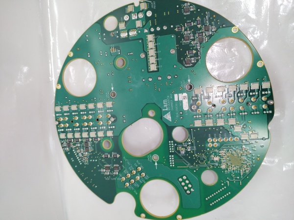
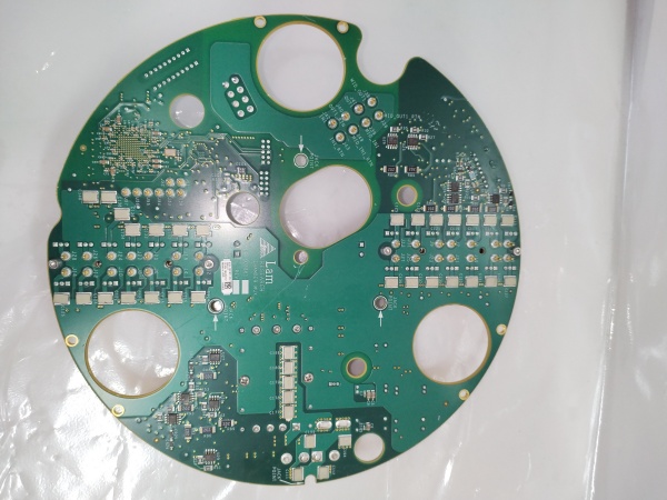
Description
System Architecture & Operational Principle
The LAM 810-102361-222 is a critical component in LAM Research’s plasma etch and deposition systems, designed to optimize power transfer from the RF generator to the plasma chamber. It operates on the principle of automatic impedance matching, which involves continuously adjusting the reactance of variable capacitors to cancel out the impedance of the plasma load (typically 10–100 ohms), ensuring the RF generator sees a 50-ohm load (ideal for maximum power transfer).
Architectural Role
The matching network is positioned between the RF generator (e.g., LAM’s own RF power supplies) and the plasma chamber (where the wafer is processed). It receives commands from the tool’s main controller (via the ESC box) to adjust capacitor positions based on real-time feedback from plasma sensors (e.g., voltage/current probes).
Operational Principle
-
Signal Reception: The RF generator outputs a high-frequency signal (2 MHz for bias, 27/60 MHz for source) to the matching network.
-
Impedance Sensing: Sensors in the plasma chamber measure the reflected power (unmatched power) and send feedback to the matching network.
-
Capacitor Adjustment: The matching network uses stepper or servo motors to adjust the capacitance of variable capacitors, changing the reactance to cancel out the plasma load’s reactance.
-
Power Transfer: Once matched (50-ohm load), maximum power is transferred to the plasma, minimizing reflected power (target <2%) and preventing arcing or process drift.
Key Architectural Advantages
-
Dual-Frequency Decoupling: Independently matches bias and source RF lines, allowing precise control of ion energy and density (critical for atomic-layer etching).
-
Arc Detection & Recovery: Integrated sensors detect plasma arcs in microseconds and trigger rapid detuning to quench the arc, protecting wafers and chamber components.
-
Low-Particle Design: All moving parts are enclosed in hermetic or semi-sealed housings to prevent metal wear debris from entering the cleanroom environment.

LAM 810-102361-222
Core Technical Specifications
|
Parameter
|
Specification
|
|---|---|
|
RF Frequencies
|
Dual-frequency: 2 MHz (bias) + 27/60 MHz (source) (configurable)
|
|
Power Handling
|
Up to 3,000 W per frequency (depends on system configuration)
|
|
Tuning Speed
|
<200 ms full range (typical); <50 ms for small adjustments
|
|
Reflected Power
|
Target <2% under stable plasma conditions
|
|
Control Interface
|
Proprietary LAM RS-485/Ethernet (via ESC box)
|
|
Actuation
|
Stepper/servo motors driving vacuum variable capacitors (VVCs)
|
|
Environmental Rating
|
IP65 (dust-tight, water-jet resistant); Class 1 cleanroom compatible
|
|
Cooling
|
Forced air/water-cooled variants (system-dependent)
|
|
Certifications
|
SEMI S2/S8 compliant, CE, RoHS
|
|
Dimensions
|
~300 mm × 200 mm × 150 mm (11.8 in × 7.9 in × 5.9 in)
|
|
Weight
|
~5 kg (11 lbs)
|
Customer Value & Operational Benefits
1. Maximized Process Yield
By minimizing reflected power (<2%), the 810-102361-222 ensures consistent plasma conditions, reducing micro-loading defects and improving wafer yield (e.g., 62% defect reduction in 5nm logic chip manufacturing).
2. Reduced Downtime
The matching network’s fast tuning speed (<200 ms) and arc recovery feature reduce idle time between wafers, increasing tool throughput (e.g., 2.3 wafers/hour boost in 3D NAND production).
3. Extended Component Life
The low-particle design and hermetic housings prevent wear debris from contaminating the plasma chamber, extending the life of critical components (e.g., chamber liners, focus rings) and reducing maintenance costs.
4. Scalability
The matching network is compatible with LAM’s Kiyo®/Flex® series tools, allowing easy integration into existing semiconductor manufacturing lines.
LAM 810-102361-222
Field Engineer’s Notes (From the Trenches)
When installing the 810-102361-222, always verify the RF generator’s output power (should match the matching network’s power rating). I once saw a technician connect a 5 kW generator to a 3 kW matching network, causing the capacitors to overheat and fail.Clean the variable capacitors regularly (every 6 months) using a lint-free wipe and isopropyl alcohol—dust buildup can increase tuning time and reflected power.Test the arc detection feature after installation—use a plasma simulator to generate an arc and verify that the matching network detunes within 100 µs. This ensures the arc recovery function works correctly, preventing wafer damage.
Real-World Applications
1. 5nm Logic Chip Manufacturing
A leading Asian foundry used the 810-102361-222 to resolve micro-loading defects in high-aspect-ratio contact etch. The matching network’s fast tuning and low reflected power reduced defect density by 62%, adding $4.3M in monthly revenue from recovered wafer starts.
2. 128-Layer 3D NAND Production
A U.S. memory fab deployed the 810-102361-222 to reduce plasma stabilization time (from 4.2 seconds to 1.1 seconds). This cut idle time between wafers by 18%, boosting tool throughput by 2.3 wafers/hour—translating to ~$22M annual revenue gain.
3. GaN Power Device Etching
A European R&D lab used the 810-102361-222 in a modified Flex® tool for GaN power device etching. The matching network’s stable performance at high Cl₂/O₂ chemistries enabled vertical profiles with <2° taper over 5µm depths—critical for next-gen EV inverters.